Four internships spanning VLSI research, physical design, RTL design, and embedded systems — at IIT-affiliated research centres, industry training institutes, and online platforms.
4
INTERNSHIPS
→
1 VLSI RESEARCH1 PHYSICAL DESIGN1 SOLAR / FSM1 RTL DESIGN
CLKDATA
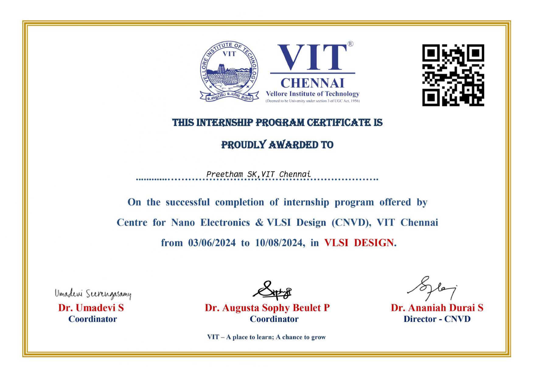
Center for Nano Electronics & VLSI Design (CNVD)
Summer Research Intern
VIT Chennai · Guide: Dr. S. Umadevi
Jun 2024 – Aug 2024
MAC UNIT
Designed a 16×16 Multiply-Accumulate (MAC) unit in Verilog HDL using Row Bypass Adder (RBA) scheme — reducing switching activity and dynamic power compared to conventional ripple carry adder based designs.
SIMULATION
Functionally verified using Cadence® NC Launch; gate-level synthesis performed using Cadence® Genus with standard cell library mapping.
OUTCOME — MAC unit architecture inspired innovation in reconfigurable binary multiplier design; resulted in Indian Patent Application No. 202541080342, published September 2025.
Verilog HDLCadence NC LaunchCadence GenusRBA DesignMAC UnitLow Power VLSI
HOVER / CLICK TO VIEW CERTIFICATE
WENSEL
Centre for Smart Grid Technologies (CSGT)
Summer Research Intern
VIT Chennai · Guide: Dr. O.V. Gnana Swathika
May 2025 – Jul 2025
FSM DESIGN
Designed an 11-state FSM-based controller for a Solar Powered EV Charging Station in Verilog HDL — managing charge states, fault detection, and power routing logic.
MPPT ALGORITHM
Implemented Perturb & Observe (P&O) MPPT algorithm for maximum solar power extraction under variable irradiance; functional simulation and waveform verification using ModelSim.
OUTCOME — Research contributed to book chapter accepted for publication — Smart Technologies for Smart Buildings, CRC Press, Taylor & Francis (ISBN: 9781041093626).
Executed complete RTL-to-GDSII physical design flow for Serial Peripheral Interface (SPI) controller using open-source Qflow EDA toolchain on OSU 0.18µm standard cell library.
IMPLEMENTATION
RTL synthesis and technology mapping (Yosys/ABC); congestion-aware placement (Graywolf); global and detailed routing (Qrouter); static timing analysis (Vesta) — 3106 cells placed, 22417 routes completed.
VERIFICATION
DRC and LVS clean verified using Magic and Netgen; fabrication-ready GDSII layout generated.
OUTCOME — Full GDSII tapeout for SPI controller. 3106 standard cells placed, 22417 routes completed, DRC ✓ LVS ✓ clean. Documented as GitHub repository with all flow stages.
Designed 5 Verilog RTL modules — UART (parameterized, FSM-based, parity-checked), synchronous FIFO (configurable width/depth), Traffic Light Controller (sensor-driven FSM with priority logic), Automatic Temperature Controller, and Washing Machine Controller.
VERIFICATION
Developed structured testbenches with stimulus generation and output monitoring; functional simulation and waveform verification using ModelSim for all 5 modules.
OUTCOME — 5 production-quality RTL modules with full testbench coverage. Documented as GitHub repository — RTL Digital Design Modules using Verilog.